| CPC H01L 25/0655 (2013.01) [H01L 23/3128 (2013.01); H01L 23/49816 (2013.01); H01L 23/49822 (2013.01); H01L 24/16 (2013.01); H01L 24/32 (2013.01); H01L 24/73 (2013.01); H01L 2224/16227 (2013.01); H01L 2224/32225 (2013.01); H01L 2224/73204 (2013.01); H01L 2924/3511 (2013.01)] | 20 Claims |
|
1. A semiconductor package, comprising:
a package substrate;
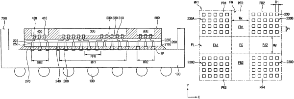
an interposer on the package substrate, the interposer including individual mounting regions on a first surface thereof and a plurality of first bonding pads in the individual mounting regions respectively;
a plurality of semiconductor devices in the individual mounting regions on the first surface of the interposer, respectively, the plurality of semiconductor devices each having chip pads electrically connected to the plurality of first bonding pads;
first conductive connection members between the plurality of first bonding pads and the chip pads; and
a molding member on the interposer, the molding member covering the plurality of semiconductor devices and filling gaps between the first surface of the interposer and the plurality of semiconductor devices, the molding member directly contacting the first surface of the interposer and a bottom surface of the plurality of semiconductor devices,
wherein at least one of the individual mounting regions includes a pad-free region with a cross shape and a plurality of pad regions defined by the pad-free region, and the plurality of first bonding pads are in the plurality of pad regions.
|