| CPC H01L 24/83 (2013.01) [H01L 24/44 (2013.01); H01L 2224/45139 (2013.01); H01L 2224/45144 (2013.01); H01L 2224/45147 (2013.01); H01L 2224/83191 (2013.01)] | 18 Claims |
|
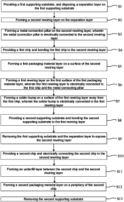
10. A three-dimensional stacked fan-out packaging structure, comprising:
a first semiconductor chip;
a first packaging material layer, comprising a first surface and a second surface opposite to the first surface, wherein the first packaging material layer is disposed in a periphery area of the first semiconductor chip;
a metal connecting pillar, disposed penetrating through the first packaging material layer;
a first rewiring layer, disposed on the first surface of the first packaging material layer, and electrically connected to the first semiconductor chip and the metal connecting pillar;
a second rewiring layer, disposed on the second surface of the first packaging material, and electrically connected to the metal connecting pillar, wherein the second rewiring layer electrically connects to the first rewiring layer through the metal connecting pillar, wherein the first semiconductor chip is bonded to the second rewiring layer;
a second semiconductor chip, disposed on a surface of the second rewiring layer away from the first semiconductor chip, and electrically connected to the second rewiring layer;
a solder ball bump, disposed on a surface of the first rewiring layer away from the first semiconductor chip, and electrically connected to the first rewiring layer;
an underfill layer, disposed between the second semiconductor chip and the second rewiring layer; and
a second packaging material layer, packaging the second semiconductor chip in a periphery area of the second semiconductor chip.
|