| CPC H01L 24/13 (2013.01) [H01L 24/03 (2013.01); H01L 24/05 (2013.01); H01L 24/11 (2013.01); H01L 2224/13027 (2013.01); H01L 2924/35 (2013.01)] | 26 Claims |

|
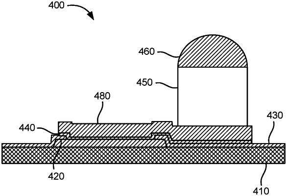
1. A flip chip connection comprising:
a substrate formed from silicon (Si);
a metal pad in direct contact with a contact side of the substrate;
a first passivation layer in direct contact with the contact side of the substrate, wherein the first passivation layer at least partially overlaps the metal pad;
a first metal layer on a contact side of the metal pad;
a metallization structure on a contact side of the first metal layer, the metallization structure comprising a redistribution layer (RDL); and
a contact structure on a contact side of the metallization structure, the contact structure comprising a copper pillar and a solder portion,
wherein widths of the copper pillar and the solder portion are equal.
|