| CPC H01L 23/528 (2013.01) [H01L 23/5226 (2013.01); H01L 29/785 (2013.01)] | 27 Claims |

|
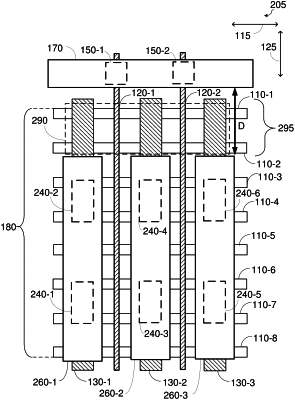
1. A die, comprising:
fins extending in a first direction;
a gate formed over the fins, the gate extending in a second direction that is perpendicular to the first direction;
a first source/drain contact layer formed over the fins and extending in the second direction;
a second source/drain contact layer formed over the fins and extending in the second direction, wherein the first source/drain contact layer and the second source/drain contact layer are on opposite sides of the gate;
a first source/drain metal layer electrically coupled to the first source/drain contact layer; and
a second source/drain metal layer electrically coupled to the second source/drain contact layer, wherein the first source/drain metal layer and the second source/drain metal layer do not overlap one or more of the fins.
|