| CPC H01L 23/49568 (2013.01) [H01L 23/3121 (2013.01); H01L 23/49537 (2013.01); H01L 23/34 (2013.01); H01L 23/49513 (2013.01); H01L 23/49562 (2013.01); H01L 23/49575 (2013.01); H01L 24/29 (2013.01); H01L 24/32 (2013.01); H01L 24/37 (2013.01); H01L 24/40 (2013.01); H01L 24/49 (2013.01); H01L 24/84 (2013.01); H01L 25/072 (2013.01); H01L 2224/29139 (2013.01); H01L 2224/32245 (2013.01); H01L 2224/40175 (2013.01); H01L 2924/1305 (2013.01); H01L 2924/181 (2013.01)] | 10 Claims |

|
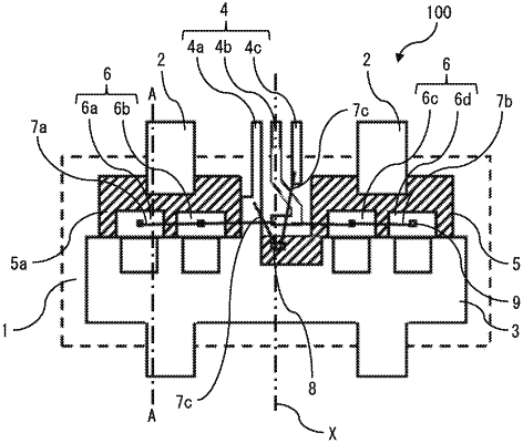
1. A semiconductor device comprising:
a heat dissipation plate formed in a plate shape;
a plurality of switching elements joined to one surface of the heat dissipation plate;
a first terminal extending in a direction away from the heat dissipation plate in a state of being apart from the heat dissipation plate, the first terminal being connected via a first electric conductor to surfaces of the plurality of switching elements on an opposite side to the heat dissipation plate side;
a sealing member sealing the plurality of switching elements, the heat dissipation plate, and the first terminal; and
a sense element disposed on the one surface of the heat dissipation plate adjacently to the notch, wherein
a notch is provided in an outer periphery portion of the heat dissipation plate, and
a portion of the first terminal on the heat dissipation plate side overlaps with a region of a cut at the notch as seen in a direction perpendicular to the one surface of the heat dissipation plate.
|