| CPC H01L 23/481 (2013.01) [H01L 21/76898 (2013.01); H01L 27/14634 (2013.01)] | 19 Claims |

|
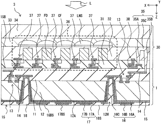
1. A semiconductor device, comprising:
a semiconductor substrate that has a first surface and a second surface on a side opposite to the first surface;
a first metal film pattern that includes a first portion and a second portion, wherein
the first portion covers a first regional portion of the first surface,
the second portion is stacked on the first portion,
the second portion is smaller in area than the first portion in a plan view such that the second portion covers a portion of an upper surface of the first portion in the plan view,
the upper surface of the first portion is parallel to the first surface of the semiconductor substrate,
the second portion includes a third surface and a fourth surface on a side opposite to the third surface, and
the third surface is substantially parallel to the fourth surface;
a second metal film pattern that includes a third portion and a fourth portion, wherein
the third portion covers a second regional portion of the first surface different from the first regional portion of the first surface, and
the fourth portion is stacked on the third portion to cover a portion of the third portion; and
an insulating layer between the second portion and the fourth portion.
|