| CPC H01L 23/481 (2013.01) [H01L 21/76898 (2013.01); H01L 23/5384 (2013.01); H01L 23/53233 (2013.01); H01L 23/53238 (2013.01); H01L 23/53252 (2013.01); H01L 23/53271 (2013.01); H01L 2223/6622 (2013.01)] | 21 Claims |

|
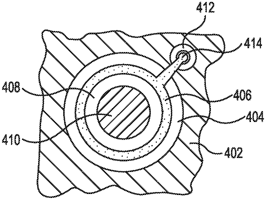
1. An apparatus, comprising:
an opening formed in a substrate, wherein the opening has at least one sidewall;
a first dielectric at least formed on the sidewall of the opening;
a first conductor at least formed on the first dielectric;
a second dielectric at least formed on the first conductor;
a second conductor at least formed on a sidewall of the second dielectric; and
a conductive coupling configured to short the first conductor to the substrate via a voltage reference node and extend across the first dielectric.
|