| CPC H01L 23/4006 (2013.01) [H01L 23/473 (2013.01); H01L 25/072 (2013.01); H01L 2023/4081 (2013.01); H01L 2023/4087 (2013.01)] | 13 Claims |

|
1. A power semiconductor module, comprising:
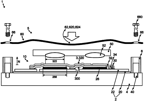
a base plate, on which a housing and a switching device enclosed by the housing are arranged;
the switching device has a substrate and a connecting device that has a first main face and a second main face;
a component group having at least three power semiconductor components is arranged on a conductor track of the substrate;
the component group defining and having a group midpoint, and having a pressure device formed on the substrate in the normal direction (N) of the pressure device in order to exert pressure;
the pressure device has a pressure body and a pressure inducing body;
a pressure element is arranged protruding from the pressure body;
the pressure element presses onto a pressure section of the second main face of the connecting device;
the pressure inducing body has a pressure transmission section with a pressure transmission point, which is approximately flush with the group midpoint in the normal direction;
a respective fastening section of the pressure inducing body is braced against the base plate to create a pressure by means of at least two fastening means which cooperate respectively with an assigned abutment of the base plate;
wherein the group midpoint is determined from the location of the power semiconductor components of a component group as the geometrical midpoint or as the force midpoint of the power semiconductor components,
wherein the pressure inducing body is configured as a two-dimensional resilient shaped metal body;
wherein the pressure transmission section is configured as a part of a connecting section or as a multiplicity of pressure transmission sections, which jut laterally out from the connecting section;
wherein a midpoint spacing from the group midpoint to the pressure transmission point is less than 0.5 times the distance of the group midpoint from the component center of that power semiconductor component of the component group which lies furthest away therefrom; and
wherein the connecting device is configured as a sheet stack having at least one electrically conductive sheet and at least one electrically insulating sheet.
|