| CPC H01L 23/3164 (2013.01) [H01L 23/3121 (2013.01); H01L 23/3135 (2013.01); H01L 23/3192 (2013.01); H01L 21/6836 (2013.01); H01L 23/295 (2013.01); H01L 24/02 (2013.01); H01L 24/05 (2013.01); H01L 24/13 (2013.01); H01L 24/16 (2013.01); H01L 24/32 (2013.01); H01L 2221/68327 (2013.01); H01L 2221/68368 (2013.01); H01L 2224/02377 (2013.01); H01L 2224/02381 (2013.01); H01L 2224/05569 (2013.01); H01L 2224/13024 (2013.01); H01L 2224/16225 (2013.01); H01L 2224/32225 (2013.01); H01L 2924/10252 (2013.01); H01L 2924/10253 (2013.01); H01L 2924/10254 (2013.01); H01L 2924/10272 (2013.01); H01L 2924/10329 (2013.01); H01L 2924/1033 (2013.01); H01L 2924/10335 (2013.01)] | 20 Claims |
|
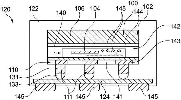
1. A package, comprising:
an electronic component that includes a dielectric layer as a base and a semiconductor die attached on top of the dielectric layer, the semiconductor die having an active area with monolithically integrated circuit elements; and
an encapsulant encapsulating the dielectric layer and the semiconductor die,
wherein the encapsulant is a mold compound having different material properties than the dielectric layer, and
wherein the electronic component further includes an adhesive layer that further promotes adhesion between the dielectric layer and the semiconductor die.
|