| CPC H01L 21/7806 (2013.01) [H01L 21/02447 (2013.01); H01L 21/02529 (2013.01); H01L 21/0254 (2013.01); H01L 21/76254 (2013.01); H01L 29/045 (2013.01); H01L 29/1608 (2013.01); H01L 29/2003 (2013.01); H01L 29/267 (2013.01)] | 13 Claims |

|
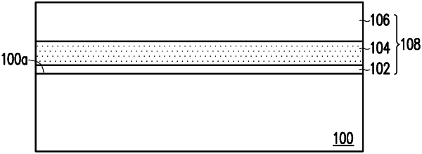
1. A semiconductor substrate, comprising:
a high-resistivity silicon carbide layer comprising a first surface and a second surface opposite to the first surface; and
a gallium nitride epitaxial layer formed on the second surface of the high-resistivity silicon carbide layer, wherein a thickness of the gallium nitride epitaxial layer is less than 2 μm, and a full width at half maximum (FWHM) of an X-ray diffraction analysis (002) plane is less than 100 arcsec, and
a thickness of the high-resistivity silicon carbide layer ranges from 20 μm to 50 μm, the second surface of the high-resistivity silicon carbide layer has an angle ranging from 0° to +/−8° with respect to a (0001) plane, a micropipe density (MPD) of the high-resistivity silicon carbide layer is less than 0.5 ea/cm2, basal plane dislocation (BPD) of the high-resistivity silicon carbide layer is less than 10 ea/cm2, and threading screw dislocation (TSD) of the high-resistivity silicon carbide layer is less than 500 ea/cm2.
|
|
10. A semiconductor substrate, comprising:
an N-type silicon carbide (N—SiC) layer; and
a gallium nitride epitaxial layer formed on a surface of the N-type silicon carbide (N—SiC) layer, wherein a thickness of the gallium nitride epitaxial layer ranges from 0.3 μm to 6 μm, and a full width at half maximum (FWHM) of an X-ray diffraction analysis (002) plane is less than 100 arcsec, and
a thickness of the N-type silicon carbide (N—SiC) layer ranges from 0.1 μm to 50 μm, and the surface of the N-type silicon carbide (N—SiC) layer comprises an angle ranging from 0° to +/−8° with respect to a (0001) plane, a micropipe density (MPD) of the N-type silicon carbide (N—SiC) layer is less than 0.5 ea/cm2, basal plane dislocation (BPD) of the N-type silicon carbide (N—SiC) layer is less than 10 ea/cm2, and threading screw dislocation (TSD) of the N-type silicon carbide (N—SiC) layer is less than 500 ea/cm2.
|