| CPC H01L 21/76823 (2013.01) [H01L 21/42 (2013.01); H01L 21/76825 (2013.01); H01L 21/76843 (2013.01)] | 12 Claims |

|
1. A method comprising:
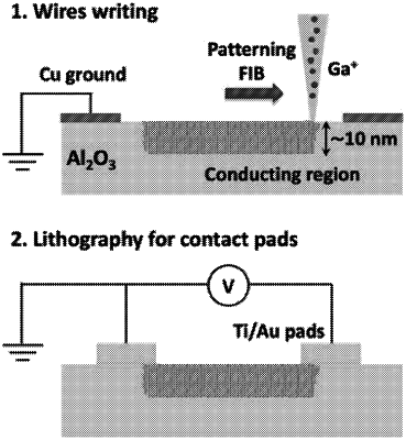
(a) irradiating a region of a dielectric material having a resistivity of at least 108 Ω cm with a focused ion beam, the irradiated region corresponding to a conductive feature embedded in the dielectric material, the conductive feature having a conductivity greater than that of the dielectric material; and
(b) forming one or more contact pads of a conductive material in electrical communication with the conductive feature, the one or more contact pads configured to apply a voltage across the conductive feature using a voltage source, the method further comprising heating the conductive feature under an oxidizing atmosphere for a period of time so as to erase the conductive feature.
|