| CPC H01L 21/02458 (2013.01) [H01L 21/02376 (2013.01); H01L 21/0254 (2013.01); H01L 21/02631 (2013.01); H01L 29/1608 (2013.01); H01L 29/2003 (2013.01); H01L 29/66462 (2013.01); H01L 29/7786 (2013.01)] | 12 Claims |

|
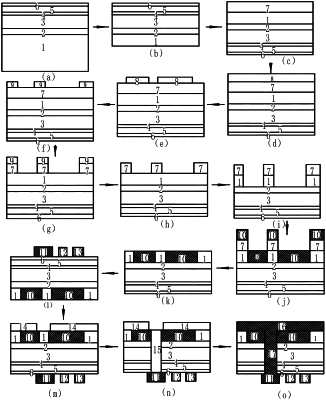
1. A preparation method of a gallium nitride (GaN) field effect transistor, comprising following steps:
step 1, preparing a GaN heterojunction layer on a front-side of a silicon carbide (SiC) substrate;
step 2, thinning a backside of the SiC substrate to obtain a thinned SiC substrate;
step 3, growing a sacrificial layer on a backside of the thinned SiC substrate;
step 4, coating a photoresist on the sacrificial layer;
step 5, exposing and developing the photoresist to form a metal mask area graphics on the sacrificial layer;
step 6, evaporating and stripping a metal on the metal mask area graphics to form a metal mask layer on the metal mask area graphics;
step 7, removing a part of the sacrificial layer that is outside an area covered by the metal mask layer to form a groove area on the sacrificial layer and to obtain a remaining sacrificial layer;
step 8, removing the metal mask layer using a wet process;
step 9, using the remaining sacrificial layer as a mask, and etching the thinned SiC substrate such that the groove area extends to a backside of the GaN heterojunction layer and to obtain a remaining SiC substrate;
step 10, growing a diamond layer on the remaining sacrificial layer and the backside of the GaN heterojunction layer;
step 11, removing a part of the diamond layer that covers the remaining sacrificial layer using the wet process to obtain a remaining diamond layer, and removing the remaining sacrificial layer using the wet process;
step 12, preparing a source electrode, a drain electrode and a gate electrode on a front-side of the GaN heterojunction layer;
step 13, preparing a through hole mask layer on the remaining diamond layer and the remaining SiC substrate;
step 14, using the through hole mask layer as a mask, and etching the remaining SiC substrate and the GaN heterojunction layer to form a source through hole that is in communication with the source electrode; and
step 15, removing the through hole mask layer, and preparing a back grounding metal on the remaining diamond layer and the remaining SiC substrate, to complete preparation of the GaN field effect transistor, the back grounding metal being in communication with the source through hole.
|