| CPC H01J 37/32532 (2013.01) [H01J 37/32082 (2013.01); H01J 37/32146 (2013.01); H01J 37/32706 (2013.01); H01J 37/32935 (2013.01); H01J 37/3299 (2013.01)] | 5 Claims |

|
1. A plasma processing apparatus, comprising:
a processing chamber in which plasma processing of a sample is carried out by using plasma;
a radio frequency power source which supplies a radio frequency power for generating the plasma;
a sample stage in which a first electrode and a second electrode which electrostatically chuck the sample are arranged and on which the sample is mounted;
a DC power source which applies a first DC voltage and a second DC voltage to the first and second electrodes, the first DC voltage being a positive DC voltage value, and the second DC voltage being a negative DC voltage value; and
a controller configured to
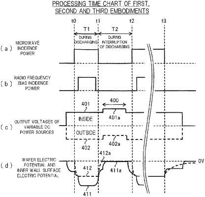
control the DC power source to apply a predetermined positive output voltage value to the first electrode during a plasma discharging period, and to apply a predetermined negative output voltage value to the second electrode during the plasma discharging period;
control the DC power source to apply the first DC voltage to the first electrode to cause the first DC voltage to be a higher voltage than the predetermined positive output voltage value to the first electrode during a stepped-up voltage time period; and
control the DC power source to apply the second DC voltage to the second electrode to cause the second DC voltage to be a higher voltage than the predetermined negative output voltage value to the second electrode during the stepped-up voltage time period such that the first DC voltage value and the second DC voltage value act in cooperation to reduce an absolute value of an electric potential of the sample during the stepped-up voltage time period which occurs within a discharge interruption time period, the discharge interruption time period occurring between two or more plasma discharging periods,
wherein the radio frequency power source does not output the radio frequency power during the discharge interruption time period,
wherein the first DC voltage value and the second DC voltage value are obtained based on a resistance value between the sample and the first electrode and a resistance value between the sample and the second electrode,
wherein the resistance value between the sample and the first electrode is different from the resistance value between the sample and the second electrode, and
wherein the stepped-up voltage time period is shorter than the discharge interruption time period, and begins after the start of the discharge interruption time period and ends before the end of the discharge interruption time period.
|