| CPC H01G 9/0036 (2013.01) [C23C 14/0694 (2013.01); C23C 14/228 (2013.01); C23C 14/50 (2013.01); C23C 14/5806 (2013.01); H01G 9/2009 (2013.01); H10K 30/30 (2023.02); H10K 30/40 (2023.02); H10K 30/82 (2023.02); H10K 71/164 (2023.02); H10K 85/30 (2023.02)] | 12 Claims |

|
1. A method of forming a perovskite precursor layer comprising:
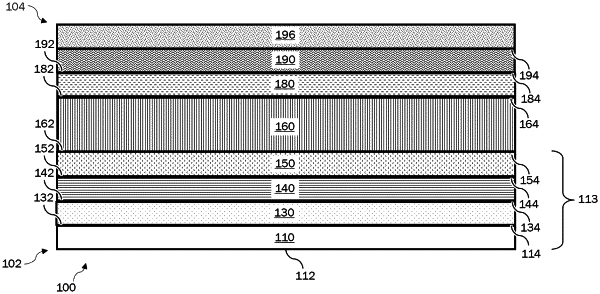
providing a substrate stack in a deposition chamber, the substrate stack having a first charge transport layer on an electrode;
depositing a first perovskite-forming composition on the substrate stack in the deposition chamber by a vapor transport deposition (VTD) process, comprising:
heating a source material to a temperature in a range of 375° C. to 550° C., wherein the source material comprises at least one of: lead iodide (PbI2), lead bromide (PbBr2), cesium bromide (CsBr), cesium lead iodide (CsPbI3), cesium tin iodide (CsSnI3), lead chloride (PbCl2), tin iodide (SnI2), tin bromide (SnBr2), or tin chloride (SnCl2);
providing a vapor curtain to direct vapor of the source material using a carrier gas toward the substrate stack in the deposition chamber, wherein the vapor curtain has a width greater than 1 meter, the deposition chamber having a pressure in a range of 0.1 to 2.0 Torr; and
forming the precursor layer, at a deposition rate in a range of 0.01 to 1.50 μm per minute, to a thickness of 100-2000 nm, wherein the precursor layer comprises a plurality of metal halide crystal grain structures, wherein: the grain structures have a height, normal to the surface of the substrate stack, and a width, parallel to the surface of the substrate stack, and an average grain width is less than a third of an average grain height.
|