| CPC H01C 1/14 (2013.01) [H01C 3/08 (2013.01); H05K 1/181 (2013.01); H05K 2201/10022 (2013.01)] | 17 Claims |
|
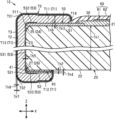
1. A chip resistor, comprising:
a substrate including an upper surface, a back surface, and a side surface, the upper surface and the back surface intersecting a thickness-wise direction, and the side surface joining the upper surface and the back surface;
an upper electrode and a resistor body formed on the upper surface;
a back electrode formed on the back surface;
a side electrode formed on the side surface; and
a metal plating layer including a back plating layer covering at least a portion of the back electrode and a side plating layer covering at least a portion of the side electrode, wherein the metal plating layer has a thickness that is greater than or equal to 10 μm and less than or equal to 60 μm, wherein
the substrate includes a corner joining the back surface and the side surface,
the corner includes an inclined surface intersecting the back surface and the side surface, and
the metal plating layer includes a portion that covers the corner and is roundly curved.
|