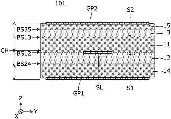
| CPC H01B 7/0838 (2013.01) [H01B 11/203 (2013.01)] | 12 Claims |

|
1. A multilayered substrate comprising:
a plurality of laminated insulating layers including a first insulating layer, a second insulating layer, a third insulating layer, a fourth insulating layer, and a fifth insulating layer; and
a transmission line; wherein
the first insulating layer includes a first surface and a second surface that are opposite to each other;
a signal conductor of the transmission line is provided on the first surface of the first insulating layer;
the second insulating layer is in contact with the first surface of the first insulating layer;
the third insulating layer is in contact with the second surface of the first insulating layer;
a dielectric loss of the second insulating layer is lower than a dielectric loss of the third insulating layer;
a degree of close contact between the first insulating layer and the third insulating layer is higher than a degree of close contact between the first insulating layer and the second insulating layer;
a material of each of the first insulating layer, the second insulating layer, and the third insulating layer is different from one another;
a boundary surface between the first insulating layer and the second insulating layer is closer to a center in a lamination direction than is a boundary surface between the first insulating layer and the third insulating layer;
the fourth insulating layer is in contact with a surface of the second insulating layer opposite to a surface with which the first insulating layer is in contact;
the fifth insulating layer is in contact with a surface of the third insulating layer opposite to a surface with which the first insulating layer is in contact;
a boundary surface between the second insulating layer and the fourth insulating layer is closer to the center in the lamination direction than is a boundary surface between the first insulating layer and the third insulating layer; and
the degree of close contact between the first insulating layer and the third insulating layer is higher than a degree of close contact between the second insulating layer and the fourth insulating layer.
|