| CPC G11C 29/42 (2013.01) [G11C 7/1069 (2013.01); G11C 7/1096 (2013.01); G11C 29/12005 (2013.01); G11C 29/4401 (2013.01)] | 20 Claims |

|
1. An apparatus, comprising:
an array of memory cells; and
a controller for access of the array of memory cells, wherein the controller is configured to cause the apparatus to:
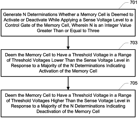
apply a sense voltage level to a control gate of a memory cell of the array of memory cells;
generate N determinations whether the memory cell is deemed to activate or deactivate while applying the sense voltage level, wherein N is an integer value greater than or equal to three;
deem the memory cell to have a threshold voltage in a first range of threshold voltages lower than the sense voltage level in response to a majority of the N determinations indicating activation of the memory cell; and
deem the memory cell to have a threshold voltage in a second range of threshold voltages higher than the sense voltage level in response to a majority of the N determinations indicating deactivation of the memory cell.
|