| CPC G11C 29/40 (2013.01) [G11C 29/30 (2013.01); G11C 2029/3202 (2013.01)] | 20 Claims |
|
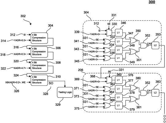
1. A method of using on-chip circuitry to test a memory of a chip, the method comprising:
in a capture stage, receiving, at a first n-bit compression structure including n first stage latches corresponding to each bit of the first n-bit compression structure, a value at each respective first stage latch for each of n memory addresses of the memory of the chip, such that each respective first stage latch receives a respective value from a memory address of the memory, n being an integer greater than one;
in the capture stage, passing the values from each respective first stage latch through compression logic of the first n-bit compression structure to output a single compressed address value, and providing the single compressed address value to a second stage latch of the first n-bit compression structure; and
in a testing stage, comparing the single compressed address value of the second stage latch of the first n-bit compression structure, as output from the first n-bit compression structure, to a desired value to determine whether an interface to the memory is operating as desired.
|