US 12,112,810 B2
Non-volatile semiconductor storage device
Naoki Matsunaga, Tokyo (JP)
Assigned to Kioxia Corporation, Tokyo (JP)
Filed by Kioxia Corporation, Tokyo (JP)
Filed on Apr. 6, 2023, as Appl. No. 18/296,430.
Application 18/296,430 is a continuation of application No. 17/373,012, filed on Jul. 12, 2021, granted, now 11,631,468.
Application 17/373,012 is a continuation of application No. 16/997,308, filed on Aug. 19, 2020, granted, now 11,069,414, issued on Jul. 20, 2021.
Application 16/997,308 is a continuation of application No. 16/354,972, filed on Mar. 15, 2019, granted, now 10,762,969, issued on Sep. 1, 2020.
Application 16/354,972 is a continuation of application No. 15/918,606, filed on Mar. 12, 2018, granted, now 10,269,436, issued on Apr. 23, 2019.
Application 15/918,606 is a continuation of application No. 15/581,904, filed on Apr. 28, 2017, granted, now 9,953,716, issued on Apr. 24, 2018.
Application 15/581,904 is a continuation of application No. 15/257,773, filed on Sep. 6, 2016, granted, now 9,666,299, issued on May 30, 2017.
Application 15/257,773 is a continuation of application No. 14/331,893, filed on Jul. 15, 2014, granted, now 9,466,370, issued on Oct. 11, 2016.
Application 14/331,893 is a continuation of application No. 13/531,791, filed on Jun. 25, 2012, granted, now 8,804,435, issued on Aug. 12, 2014.
Claims priority of application No. 2011-269942 (JP), filed on Dec. 9, 2011.
Prior Publication US 2023/0260578 A1, Aug. 17, 2023
This patent is subject to a terminal disclaimer.
Int. Cl. G11C 7/00 (2006.01); G06F 3/06 (2006.01); G06F 11/10 (2006.01); G11C 11/56 (2006.01); G11C 16/04 (2006.01); G11C 16/06 (2006.01); G11C 16/26 (2006.01); G11C 16/34 (2006.01); G11C 29/52 (2006.01)
CPC G11C 16/26 (2013.01) [G06F 3/0619 (2013.01); G06F 3/064 (2013.01); G06F 3/0655 (2013.01); G06F 3/0679 (2013.01); G06F 11/1068 (2013.01); G11C 11/5628 (2013.01); G11C 11/5642 (2013.01); G11C 16/04 (2013.01); G11C 16/0483 (2013.01); G11C 16/06 (2013.01); G11C 16/3404 (2013.01); G11C 16/349 (2013.01); G11C 16/3495 (2013.01); G11C 29/52 (2013.01)] 7 Claims
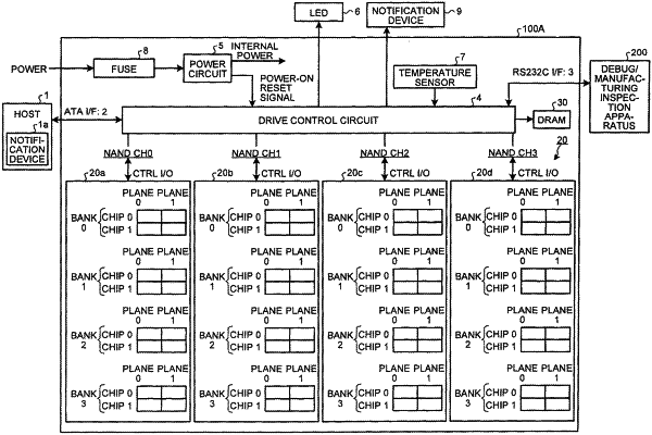
OG exemplary drawing
 
1. An information processing apparatus connectable to a memory system, the information processing apparatus comprising:
a display device; and
a processor configured to transmit a read request to the memory system,
wherein the memory system includes:
a nonvolatile memory; and
a controller circuit configured to:
receive the read request from the information processing apparatus;
on receiving the read request, perform a read processing until the read processing succeeds, the read processing including a first read operation and one or more second read operation, the first read operation including reading data from the nonvolatile memory with a first parameter, the second read operation including reading the data from the nonvolatile memory with a second parameter that is different from the first parameter; and
if a number of the first and second read operations exceeds a first threshold, transmit, to the information processing apparatus, information about a life of the nonvolatile memory based on the number of the first and second read operations,
wherein the processor is further configured to:
receive, from the memory system, the information about the life of the nonvolatile memory; and
cause the display device to display the life of the nonvolatile memory.