| CPC G11C 16/10 (2013.01) [G11C 16/0483 (2013.01); H10B 41/10 (2023.02); H10B 41/27 (2023.02); H10B 41/35 (2023.02); H10B 43/10 (2023.02); H10B 43/27 (2023.02); H10B 43/35 (2023.02)] | 45 Claims |

|
1. An apparatus, comprising:
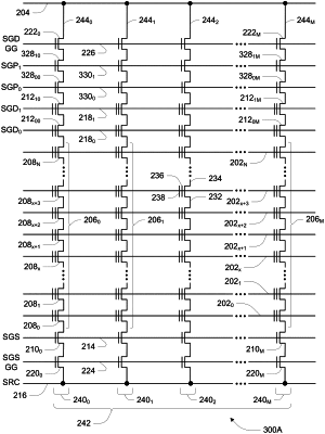
an array of memory cells comprising a plurality of strings of series-connected memory cells;
a data line;
a first set of field-effect transistors between the data line and a first string of series-connected memory cells of the plurality of strings of series-connected memory cells, wherein each field-effect transistor of the first set of field-effect transistors is connected in series between the data line and the first string of series-connected memory cells;
a second set of field-effect transistors between the data line and a second string of series-connected memory cells of the plurality of strings of series-connected memory cells, wherein each field-effect transistor of the second set of field-effect transistors is connected in series between the data line and the second string of series-connected memory cells;
a first select line connected to a control gate of a respective field-effect transistor of the first set of field-effect transistors, and to a control gate of a respective field-effect transistor of the second set of field-effect transistors, corresponding to a first position of the first binary permutation of two threshold voltages and of the second binary permutation of two threshold voltages; and
a second select line connected to a control gate of a respective field-effect transistor of the first set of field-effect transistors, and to a control gate of a respective field-effect transistor of the second set of field-effect transistors, corresponding to a second position of the first binary permutation of two threshold voltages and of the second binary permutation of two threshold voltages;
wherein the first set of field-effect transistors was fabricated to have a first binary permutation of two threshold voltages; and
wherein the second set of field-effect transistors was fabricated to have a second binary permutation of two threshold voltages different than the first binary permutation of two threshold voltages.
|