| CPC G11C 11/5628 (2013.01) [G11C 11/5642 (2013.01); G11C 11/5671 (2013.01); G11C 16/0483 (2013.01); G11C 16/10 (2013.01); G11C 16/26 (2013.01); G11C 16/3459 (2013.01); G11C 2216/14 (2013.01)] | 21 Claims |

|
1. A memory device comprising:
a memory block including a plurality of physical pages each of which includes a plurality of memory cells;
a peripheral circuit configured to receive one logical page data among a plurality of logical page data from a memory controller, perform a first program operation to a selected physical page among the plurality of physical pages using the one logical page data, receive remaining logical page data except for the one logical page data among the plurality of logical page data from the memory controller after the first program operation, and a second program operation to the selected physical page using the remaining logical page data, wherein the first program operation and the second program operation are operations of storing data in select memory cells connected to a selected word line among the plurality of memory cells; and
a program operation controller configured to control the first program operation and the second program operation,
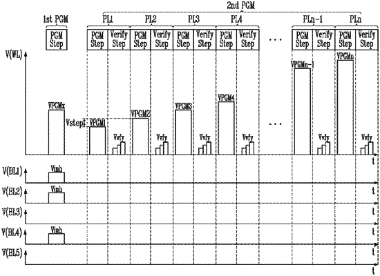
wherein the first program operation includes a program pulse apply step of applying a fixed program voltage having a predetermined voltage level to the selected word line only once, and excludes a verify step,
wherein the second program operation includes a plurality of program loops each including a program voltage apply step of applying a program voltage to a word line to which the select memory cells are commonly connected and the verify step of verifying target program states of the select memory cells, and
wherein the fixed program voltage has a level greater by an offset voltage than a voltage applied to the word line in a first program loop among the plurality of program loops.
|