| CPC G11C 11/418 (2013.01) [G11C 11/413 (2013.01); H03K 19/01742 (2013.01)] | 19 Claims |

|
1. A memory device comprising:
a memory cell configured to store data based on a first voltage;
a row decoder configured to select a wordline of the memory cell based on the first voltage; and
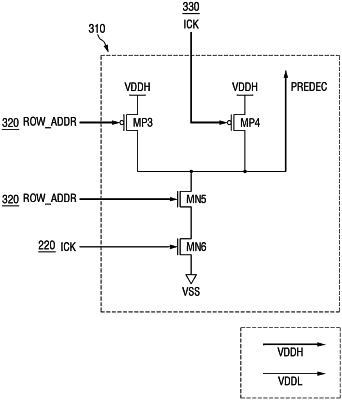
a wordline predecoder configured to generate a “predec” signal associated with generating a wordline voltage to be provided to the row decoder,
wherein the wordline predecoder is
configured to be driven by the first voltage and by a second voltage which is different from the first voltage,
configured to receive a row address signal associated with selecting the wordline, and to receive an internal clock signal associated with adjusting operating timings of elements included in the memory device,
configured to perform a NAND operation on the row address signal and the internal clock signal, and
configured to provide the “predec” signal generated based on a result of the NAND operation to the row decoder, wherein
the performing the NAND operation includes concurrently providing the first voltage to a gate of a first pull-up transistor of a NAND gate, a gate of a second pull-up transistor of the NAND gate, and a gate of a first pull-down transistor of the NAND gate, concurrently with providing the second voltage to a gate of a second pull-down transistor of the NAND gate.
|