| CPC G11C 11/4076 (2013.01) [G06F 13/1673 (2013.01); G11C 11/4096 (2013.01); H03K 19/20 (2013.01)] | 26 Claims |

|
1. An apparatus comprising:
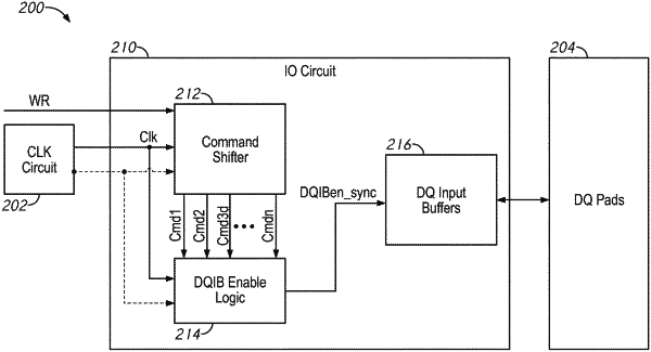
data buffer enable logic configured to provide a first intermediate data buffer enable signal and a second intermediate data buffer signal in series responsive to a first command and a second command received in series and output a combined data buffer enable signal when a gap between the first intermediate data buffer enable signal and the second intermediate data buffer enable signal is less than a predetermined period of time wherein the data buffer enable logic comprises:
a first shifter which includes a plurality of latches in series, each configured to provide one of a plurality of internal command signals; and
a logic gate configured to provide the first and the second intermediate data buffer enable signal based on the plurality of internal command signals.
|