| CPC G11C 11/161 (2013.01) [H01L 23/528 (2013.01); H10B 61/00 (2023.02); H10N 50/10 (2023.02); H10N 50/20 (2023.02); H10N 50/80 (2023.02); H10N 50/85 (2023.02)] | 18 Claims |

|
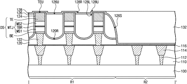
1. A magnetic memory device, comprising:
a substrate including a first region and a second region;
a first interlayer insulating layer on the substrate;
a first capping layer on the first interlayer insulating layer, the first capping layer covering the first and second regions of the substrate;
a second interlayer insulating layer on a portion of the first capping layer covering the first region of the substrate;
a bottom electrode contact included in the second interlayer insulating layer;
a magnetic tunnel junction pattern on the bottom electrode contact;
a top electrode on a top surface of the magnetic tunnel junction pattern;
a bottom electrode on a bottom surface of the magnetic tunnel junction pattern;
a second capping layer on the second interlayer insulating layer, the second capping layer being in direct contact with the first capping layer on the second region of the substrate;
third interlayer insulating layer on the second capping layer;
an upper capping layer on the third interlaver insulating layer, the upper capping layer covering the first and second regions of the substrate;
a fourth interlayer insulating layer on the upper capping layer, the fourth interlayer insulating layer covering the first and second regions of the substrate;
an upper interconnection line, the upper interconnection line penetrating the fourth interlayer insulating layer, the upper capping layer, and the second capping layer; and
a top surface of the top electrode is exposed through the second capping layer and the third interlayer insulating layer.
|