| CPC G09G 3/3266 (2013.01) [G09G 3/20 (2013.01); G11C 19/20 (2013.01); G11C 19/28 (2013.01); G09G 3/3233 (2013.01); G09G 2300/0426 (2013.01); G09G 2300/0819 (2013.01); G09G 2300/0842 (2013.01); G09G 2300/0861 (2013.01); G09G 2310/0286 (2013.01); G09G 2310/061 (2013.01); G09G 2310/08 (2013.01)] | 20 Claims |

|
1. A display panel, comprising:
a pixel circuit, including a driving transistor; and
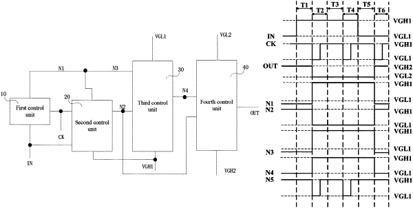
a driving circuit, configured to provide a signal for the pixel circuit, receive a third voltage signal and a fourth voltage signal, and generate an output signal, the third voltage signal being a high-level signal, and the fourth voltage signal being a low-level signal;
wherein:
a working process of the pixel circuit includes a reset phase and a separate bias phase;
the output signal of the driving circuit is a reset signal in the reset phase;
the output signal of the driving circuit is a bias signal in the bias phase; and
in response to the driving transistor being a P-type transistor, the reset signal is the fourth voltage signal, and the bias signal is the third voltage signal; or
in response to the driving transistor being an N-type transistor, the reset signal is the third voltage signal, and the bias signal is the fourth voltage signal.
|