| CPC G09G 3/325 (2013.01) [G09G 2320/046 (2013.01); G09G 2330/021 (2013.01)] | 7 Claims |

|
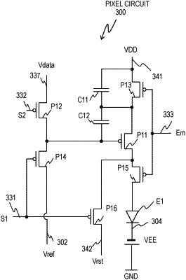
1. A pixel circuit configured to control light emission of a light-emitting element, the pixel circuit comprising:
a light-emitting element;
a driving transistor configured to control driving current for the light-emitting element;
a first capacitive element and a second capacitive element connected in series between a gate of the driving transistor and a positive power line;
a first switching transistor configured to switch connection/disconnection between the gate of the driving transistor and a data line;
a second switching transistor configured to switch supply/non-supply of electric current from the positive power line to the driving transistor;
a connection line connecting an intermediate node located between the driving transistor and the second switching transistor and an intermediate node located between the first capacitive element and the second capacitive element;
a third switching transistor configured to switch connection/disconnection between the gate of the driving transistor and a reference power line;
a fourth switching transistor configured to switch supply/non-supply of electric current from the driving transistor to the light-emitting element; and
a fifth switching transistor configured to switch connection/disconnection between a reset power line and an intermediate node located between the driving transistor and the fourth switching transistor,
wherein, during an initialization period, the first switching transistor is OFF and the second switching transistor, the third switching transistor, the fourth switching transistor, and the fifth switching transistor are ON,
wherein, during a threshold compensation period following the initialization period, the third switching transistor and the fifth switching transistor are ON and the first switching transistor, the second switching transistor, and the fourth switching transistor are OFF,
wherein, during a data write period following the threshold compensation period, the first switching transistor is ON and the second switching transistor, the third switching transistor, the fourth switching transistor, and the fifth switching transistor are OFF, and
wherein, during an emission period following the data write period, the second switching transistor and the fourth switching transistor are ON and the first switching transistor, the third switching transistor, and the fifth switching transistor are OFF.
|