| CPC G09G 3/3233 (2013.01) [H10K 59/131 (2023.02); G09G 2300/0426 (2013.01); G09G 2300/0819 (2013.01); G09G 2300/0842 (2013.01); G09G 2300/0861 (2013.01); G09G 2310/08 (2013.01)] | 20 Claims |
|
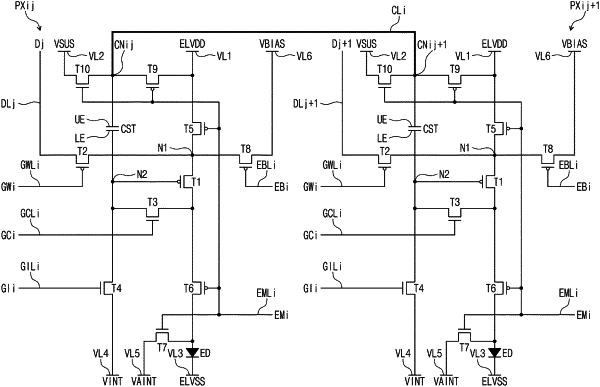
1. A display device comprising:
a display panel including:
a first pixel;
a second pixel; and
a connection line electrically connecting the first pixel and the second pixel, wherein
each of the first pixel and the second pixel includes:
a light emitting element;
a first transistor including a first electrode, a second electrode electrically connected to the light emitting element, and a gate electrode;
a second transistor electrically connected between a first driving voltage line and a connection node and including a gate electrode electrically connected to an emission line;
a third transistor electrically connected between a second driving voltage line and the connection node and including a gate electrode electrically connected to the emission line;
a fifth transistor electrically connected between the second transistor and the first electrode of the first transistor and including a gate electrode electrically connected to the emission line; and
a capacitor electrically connected between the gate electrode of the first transistor and the connection node, and
the connection node of the first pixel is electrically connected to the connection node of the second pixel through the connection line.
|