| CPC G09G 3/035 (2020.08) [G09G 3/20 (2013.01); H01L 24/05 (2013.01); H01L 24/06 (2013.01); H01L 24/48 (2013.01); H01L 25/0657 (2013.01); H01L 27/1218 (2013.01); H01L 27/124 (2013.01); G09G 2300/0426 (2013.01); H01L 2224/05573 (2013.01); H01L 2224/06145 (2013.01); H01L 2224/48145 (2013.01); H01L 2225/06506 (2013.01)] | 15 Claims |

|
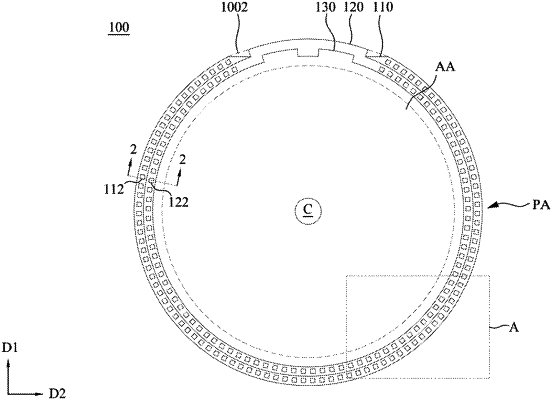
1. A display device having a display region and a periphery region surrounding the display region, wherein the display device comprises:
a driving circuit substrate comprising a plurality of first conductive pads;
a TFT array substrate comprising a plurality of second conductive pads and a plurality of data lines extending along a first direction, wherein the TFT array substrate is located on the driving circuit substrate, the data lines are electrically connected with a portion of the second conductive pads, and the portion of the second conductive pads are located at opposite two sides of the display device along the first direction;
a front plane laminate comprising a display medium layer, wherein the TFT array substrate is located between the driving circuit substrate and the front plane laminate; and
a plurality of conductive wires electrically connected with the first conductive pads and the second conductive pads respectively, wherein the first conductive pads and the second conductive pads are located in the periphery region.
|