US 12,112,398 B2
Disaggregation of system-on-chip (SOC) architecture
Naveen Matam, Rancho Cordova, CA (US); Lance Cheney, El Dorado Hills, CA (US); Eric Finley, Ione, CA (US); Varghese George, Folsom, CA (US); Sanjeev Jahagirdar, Folsom, CA (US); Altug Koker, El Dorado Hills, CA (US); Josh Mastronarde, Sacramento, CA (US); Iqbal Rajwani, Roseville, CA (US); Lakshminarayanan Striramassarma, Folsom, CA (US); Melaku Teshome, El Dorado Hills, CA (US); Vikranth Vemulapalli, Folsom, CA (US); and Binoj Xavier, Folsom, CA (US)
Assigned to Intel Corporation, Santa Clara, CA (US)
Filed by Intel Corporation, Santa Clara, CA (US)
Filed on Sep. 20, 2023, as Appl. No. 18/470,652.
Application 18/470,652 is a continuation of application No. 18/455,128, filed on Aug. 24, 2023.
Application 18/455,128 is a continuation of application No. 17/674,781, filed on Feb. 17, 2022, granted, now 11,756,150, issued on Sep. 12, 2023.
Application 17/674,781 is a continuation of application No. 17/500,375, filed on Oct. 13, 2021, granted, now 11,763,416, issued on Sep. 19, 2023.
Application 17/500,375 is a continuation of application No. 17/069,188, filed on Oct. 13, 2020, granted, now 11,410,266, issued on Aug. 9, 2022.
Application 17/069,188 is a continuation of application No. 16/355,377, filed on Mar. 15, 2019, granted, now 10,803,548, issued on Oct. 13, 2020.
Prior Publication US 2024/0013338 A1, Jan. 11, 2024
Int. Cl. G06T 1/20 (2006.01); G06F 13/40 (2006.01)
CPC G06T 1/20 (2013.01) [G06F 13/4027 (2013.01)] 20 Claims
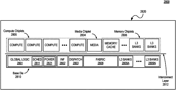
OG exemplary drawing
 
1. An apparatus comprising:
a package assembly including:
a first base chiplet comprising:
a first interconnect fabric, and
a first plurality of cache banks coupled to or integrated with the first interconnect fabric;
a first logic chiplet stacked on the first base chiplet, the first logic chiplet comprising:
a cluster of compute units to perform parallel execution of compute shader instructions or graphics shader instructions;
a first interconnect structure to couple the cluster of compute units to the first interconnect fabric;
a second base chiplet coupled to the first base chiplet by a second interconnect structure, the second base chiplet comprising:
a second interconnect fabric, and
a second plurality of cache banks coupled to or integrated with the second interconnect fabric;
a second logic chiplet stacked on the second base chiplet, the second logic chiplet comprising:
a plurality of application processor cores to execute instructions; and
a third interconnect structure to couple the second logic chiplet to the second interconnect fabric,
wherein the first logic chiplet is manufactured using a different process technology than that used to manufacture the first and second base chiplets.