| CPC G06F 30/396 (2020.01) [H01L 27/0207 (2013.01); G06F 2115/02 (2020.01); G06F 2119/22 (2020.01)] | 10 Claims |
|
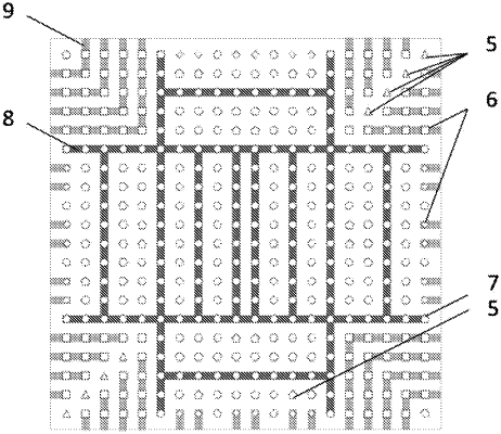
1. A wafer substrate with standard integration zones suitable for on-chip integration, wherein the wafer substrate comprises the standard integration zones, the standard integration zones are provided with pins upwards, an on-chip routing network is constructed by connecting the pins, and the standard integration zones are routed by a semiconductor machine, and wherein each standard integration zone comprises:
a top metal layer comprising core voltage pins, interconnection signal pins and function pins,
a middle metal layer comprising clock signal pins, and
a bottom metal layer comprising ground pins;
wherein the wafer substrate further comprises a core voltage network, an interconnection signal network, a clock signal network and a ground network;
wherein the core voltage network is constructed by connecting the core voltage pins and is configured to acquire the core voltage power supply capability;
wherein the interconnection signal network is constructed by connecting the interconnection signal pins distributed in different standard integration zones and is configured to provide interconnection channels for different standard integration zones;
wherein the clock signal network is constructed by connecting the clock signal pins;
wherein the ground network is constructed by connecting the ground pins; and
wherein the standard integration zones are separately communicated with external signals by the function pins for system testing and multi-domain power supply.
|