| CPC G06F 30/367 (2020.01) | 10 Claims |

|
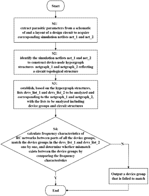
1. A method for analyzing a static analog integrated circuit layout, comprising steps of:
S1: extracting parasitic parameters from a schematic of and a layout of a design circuit to acquire corresponding simulation netlists net_1 and net_2;
S2: identifying the simulation netlists net_1 and net_2 to construct device-node hypergraph or graph structures netgraph_1 and netgraph_2 reflecting a circuit topological structure;
S3: establishing, based on the device-node hypergraph or graph structures, lists devs_list_1 and devs_list_2 to be analyzed and corresponding to the netgraph_1 and netgraph_2, wherein the lists to be analyzed comprise device groups and circuit structures; and
S4: calculating frequency characteristics of RC networks between ports of all the device groups, matching the device groups in the devs_list_1 and devs_list_2 one by one, and determining whether mismatch exists between the device groups by comparing the frequency characteristics;
wherein in S4, calculating the frequency characteristics of the RC networks comprises steps of:
S401: providing an independent AC unit source current at i-ports of the RC networks;
S402: performing frequency scanning on each of the RC networks; and
S403: storing node voltage values of j-ports in each frequency point, and performing analysis to acquire a frequency-impedance list.
|