| CPC G06F 3/0659 (2013.01) [G06F 3/0604 (2013.01); G06F 3/0656 (2013.01); G06F 3/0679 (2013.01); G11C 16/0483 (2013.01); G11C 11/56 (2013.01)] | 18 Claims |
|
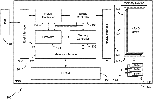
1. A memory storage system comprising:
a non-volatile semiconductor memory device comprising a memory array, a first plurality of buffers, and a second plurality of buffers, wherein the first plurality of buffers are configured to hold data prior to being encoded for storage in the memory array and the second plurality of buffers are configured to hold encoded data for storage in the memory array;
a non-volatile memory interface coupled to the non-volatile semiconductor memory device; and
a controller in communication with the first plurality of buffers and the second plurality of buffers, the controller configured to:
effectuate a transfer a plurality of data payloads to the first plurality of buffers via the non-volatile memory interface, the plurality of data payloads corresponding to data prior to being encoded for storage in the memory array;
issue a read command via the non-volatile memory interface to the non-volatile semiconductor memory device for data associated with the plurality of data payloads; and
in response to the read command, effectuate a transfer of the data associated with the data payloads out of the first plurality of buffers via the non-volatile memory interface.
|