| CPC G06F 3/0443 (2019.05) [G02F 1/136204 (2013.01); G02F 1/136286 (2013.01); G02F 1/1368 (2013.01)] | 11 Claims |

|
1. An active matrix substrate comprising:
a plurality of scanning lines;
a plurality of data lines disposed to intersect the plurality of scanning lines;
a plurality of thin-film transistors disposed separately in each of a plurality of pixels demarcated by the plurality of scanning lines and the plurality of data lines; and
a plurality of pixel electrodes connected to the plurality of thin-film transistors,
wherein
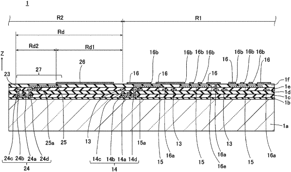
the active matrix substrate has, in a plan view, a pixel region where the plurality of pixel electrodes is provided and a frame region surrounding the pixel region,
the active matrix substrate further comprises:
a touch electrode disposed to face the plurality of pixel electrodes in the pixel region,
a frame touch electrode formed at a first layer in the frame region and not electrically connected to the touch electrode, and
a semiconductor, formed at a second layer different from the first layer in the frame region, that intersects at least one of the plurality of scanning lines connecting at least one of the plurality of pixels, or that intersects a gate electrode branching off from the at least one of the plurality of scanning lines, and
the frame region comprises:
a first region, provided in a position adjacent to the pixel region, where the frame touch electrode is disposed, and
a second region, provided in a position opposite to the pixel region across the first region, where the frame touch electrode is not disposed but the semiconductor is disposed.
|