| CPC G06F 21/44 (2013.01) [G06F 13/20 (2013.01); G06F 21/85 (2013.01); H04L 12/40 (2013.01); H04L 2012/40215 (2013.01); H04L 2012/40273 (2013.01)] | 20 Claims |

|
1. An apparatus, comprising:
processing circuitry; and
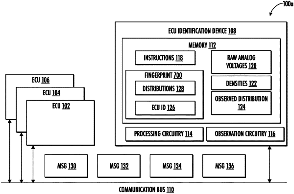
memory coupled to the processing circuitry, the memory comprising instructions that when executed by the processing circuitry cause the processing circuitry to:
process a voltage waveform of a message from a communication bus;
determine a message identification (MID) from the message;
determine if the memory comprises a fingerprint associated with the MID;
generate a set of histograms from the voltage waveform after a failure to find the fingerprint associated with the MID in the memory;
generate a density from the set of histograms with a kernel based density function, the kernel based density function to fit the set of histograms as a sum of kernels;
generate an observed distribution from the density of the voltage waveform with a cumulative distribution function (CDF); and
store the fingerprint with an indicator of the MID in the memory to associate the MID with the fingerprint, wherein the fingerprint comprises an indication of the observed distribution.
|