| CPC G06F 13/30 (2013.01) [G06F 13/1668 (2013.01)] | 20 Claims |

|
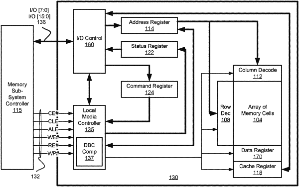
1. A memory device comprising:
a memory array; and
processing logic, operatively coupled with the memory array, to perform operations comprising:
causing a data burst to be initiated by toggling a logical level of a control pin from a first level corresponding to a data burst inactive mode to a second level corresponding to a data burst active mode, wherein the data burst corresponds to a data transfer across an interface bus;
causing the data burst to be suspended by toggling the logical level of the control pin from the second level to a third level corresponding to a data burst suspend mode; and
causing the data burst to be resumed by toggling the logical level of the control pin from the third level to the second level.
|