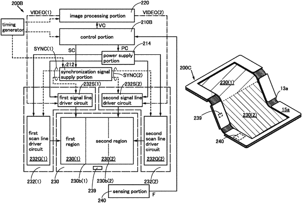
| CPC G06F 1/1652 (2013.01) [G06F 3/041 (2013.01); G06F 2203/04102 (2013.01)] | 6 Claims |

|
1. A display device comprising:
a hinge;
a sensing portion;
a magnet;
a display panel, the display panel comprising:
a substrate;
a first gate electrode of a transistor over the substrate;
a first insulating film over the first gate electrode;
a second insulating film over the first insulating film;
an oxide semiconductor film over the second insulating film;
a first conductive film and a second conductive film electrically connected to the oxide semiconductor film;
a third insulating film over the oxide semiconductor film, the first conductive film, and the second conductive film;
a second gate electrode of the transistor over the third insulating film, the second gate electrode of the transistor overlapping with the first gate electrode; and
a light-emitting element electrically connected to the transistor;
a first support panel overlapping with the display panel;
a second support panel overlapping with the display panel;
a third support panel overlapping with the first support panel;
a first member overlapping with the display panel and the first support panel; and
a second member overlapping with the third support panel,
wherein the first member is provided between the first support panel and the display panel,
wherein the sensing portion overlaps with the first support panel,
wherein the magnet overlaps with the second support panel,
wherein the display panel comprises a first display region overlapping with the first support panel, a second display region overlapping with the second support panel, and a third display region overlapping with the hinge,
wherein each of the first display region, the second display region, and the third display region is not visible by a user in a folded state of the display device,
wherein, in an opened state of the display device, the third display region is provided between the first display region and the second display region,
wherein the display device is configured to be bent in the third display region,
wherein the third support panel is provided on a display side of the display panel and around the first display region,
wherein the second member is provided on the display side of the display panel and around a part of the first display region, a part of the second display region, and a part of the third display region,
wherein, in the folded state of the display device, the display device is configured to keep the folded state by using magnetic force of the magnet,
wherein, in the opened state of the display device, the first display region, the second display region, and the third display region are visible by the user, and
wherein, in the folded state of the display device, the first display region faces the second display region.
|