| CPC G06F 1/08 (2013.01) [H04L 25/03057 (2013.01)] | 20 Claims |

|
1. A memory device, comprising:
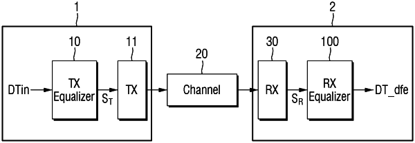
a receiving circuit, the receiving circuit including:
a first path receiving a received signal, and outputting the received signal directly as a first corrected signal in a current clock signal;
a second path holding or tracking the received signal, and outputting a second corrected signal in the current clock signal,
wherein the second corrected signal is held in a previous clock signal;
a summing circuit summing the first corrected signal and the second corrected signal, and outputting a summed received signal; and
a decision feedback equalizer comparing the summed received signal with a reference signal to decide equalized data, and outputting the equalized data in the current clock signal.
|