US 12,111,581 B2
Method to manufacture nano ridges in hard ceramic coatings
Mehmet Ali Akbas, Cheshire, CT (US); Tammo Uitterdijk, Wilton, CT (US); Christopher John Mason, Newtown, CT (US); Matthew Lipson, Stamford, CT (US); David Hart Peterson, Milford, CT (US); Michael Perry, Thomaston, CT (US); Peter Helmus, New Milford, CT (US); Jerry Jianguo Deng, Ridgefield, CT (US); and Damoon Sohrabibabaheidary, Norwalk, CT (US)
Assigned to ASML Holding N.V., Veldhoven (NL)
Appl. No. 17/291,086
Filed by ASML Holding N.V., Veldhoven (NL)
PCT Filed Oct. 22, 2019, PCT No. PCT/EP2019/078691
§ 371(c)(1), (2) Date May 4, 2021,
PCT Pub. No. WO2020/094387, PCT Pub. Date May 14, 2020.
Claims priority of provisional application 62/755,786, filed on Nov. 5, 2018.
Prior Publication US 2021/0405539 A1, Dec. 30, 2021
Int. Cl. G03F 7/20 (2006.01); G03F 7/00 (2006.01); H01L 21/687 (2006.01)
CPC G03F 7/707 (2013.01) [G03F 7/70491 (2013.01); H01L 21/6875 (2013.01)] 18 Claims
OG exemplary drawing
 
1. A method for reducing sticking of a wafer to a wafer support used in a lithography process, wherein the wafer support comprises a plurality of burls and each of the plurality of burls has a surface configured to support a back surface of the wafer, the method comprising:
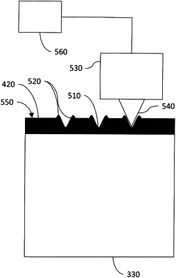
receiving, at a control computer, instructions for a tool configured to modify the surfaces of the plurality of burls; and
forming, in a deterministic manner based on the instructions received at the control computer, the modified surfaces of the plurality of burls with a furrow and a ridge,
wherein the ridge reduces the sticking by reducing a contact surface area of the modified surfaces of the plurality of burls.