| CPC G03F 1/36 (2013.01) [G06F 30/20 (2020.01)] | 8 Claims |
|
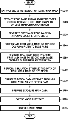
1. A method for performing optical proximity correction (OPC) comprising:
extracting edges for a layout of a pattern on a mask;
extracting edge pairs for the layout of the pattern on the mask itself in which widths between adjacent edges among the edges are equal to or less than a certain distance;
generating a coupling edge for each of the edge pairs;
generating a first mask image by applying an edge filter to the edges; and
correcting the first mask image by applying a coupling filter to the coupling edge,
wherein edge filter corresponds to a first difference image obtained by subtracting a thin mask image obtained through a thin mask approximation from a rigorous mask image obtained through an electromagnetic field simulation in an edge portion of a pattern comprising the edge pairs, and
wherein the coupling filter corresponds to a second difference image obtained by subtracting the first difference image and the thin mask image from the rigorous mask image for the mask pattern.
|