| CPC G02F 1/1368 (2013.01) [G02F 1/133357 (2021.01); G02F 1/13338 (2013.01); G02F 1/134363 (2013.01); G02F 1/136209 (2013.01); G02F 1/136227 (2013.01); G02F 1/136286 (2013.01)] | 20 Claims |

|
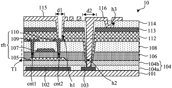
1. An array substrate, comprising:
a substrate;
a light-shielding layer disposed on the substrate;
a touch trace disposed on the substrate; and
a data line, wherein the data line and the touch trace are disposed on different layers, and at least one of the data line and the touch trace is disposed on a same layer as the light-shielding layer, wherein an orthographic projection of the data line on the substrate partially covers an orthographic projection of the touch trace on the substrate, and the orthographic projection of the data line on the substrate and the orthographic projection of the touch trace on the substrate are partially staggered;
wherein the array substrate further comprises:
a first via hole;
a second via hole, wherein a width of an aperture of the first via hole is smaller than a width of an aperture of the second via hole;
a thin film transistor structure layer including a thin film transistor and the data line, wherein the thin film transistor is disposed on the substrate, and the light-shielding layer shields the thin film transistor;
a planarization layer disposed on a side of the thin film transistor structure layer away from the substrate;
a first electrode disposed on a side of the planarization layer away from the substrate;
a connection electrode, wherein the first electrode is connected to the touch trace through the connection electrode;
a third via hole, wherein the first electrode is disposed on the planarization layer, the thin film transistor includes a source electrode and a drain electrode, wherein the source electrode and the drain electrode are disposed on a same layer as the data line;
a passivation layer disposed on a side of the first electrode away from the thin film transistor structure layer, wherein the first via hole penetrates through the passivation layer and the planarization layer; the second via hole penetrates through the passivation layer, the planarization layer, and an insulating layer of the thin film transistor structure layer; and the third via hole penetrates through the passivation layer; wherein the connection electrode is disposed on the passivation layer and extends into the second via hole and the third via hole, an end of the connection electrode is connected to the touch trace, and another end of the connection electrode is connected to the first electrode; and
a second electrode disposed on the passivation layer, wherein the connection layer is disposed on a same layer as the second electrode, and the second electrode is connected to the drain electrode through the first via hole.
|