| CPC G02F 1/133603 (2013.01) [G02F 1/133607 (2021.01)] | 20 Claims |

|
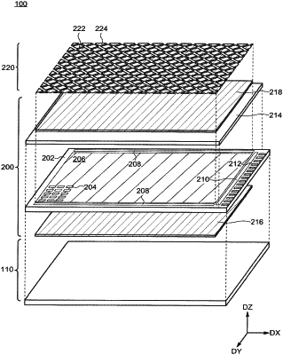
1. A light source device comprising:
a housing body;
a light source substrate located over and accommodated in the housing body;
a plurality of inorganic light-emitting elements over the light source substrate;
an optical sheet located over the plurality of inorganic light-emitting elements, accommodated in the housing body, and spaced away from the light source substrate; and
at least one spacer accommodated in the housing body and in direct contact with a bottom surface of the optical sheet,
wherein a first region of an upper surface of the light source substrate overlaps all of the plurality of inorganic light-emitting elements, and a second region of an upper surface of the light source substrate outside the first region overlaps the at least one spacer,
the at least one spacer includes:
a first supporting layer; and
a second supporting layer over and in contact with the first supporting layer, and the first supporting layer and the second supporting layer respectively include a first material and a second material different from each other.
|