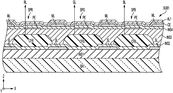
| CPC G02F 1/133526 (2013.01) [G02F 1/133345 (2013.01); G02F 1/133621 (2013.01); G02F 1/134363 (2013.01); G02F 1/136222 (2021.01); G02F 1/136286 (2013.01); G02F 2201/52 (2013.01)] | 5 Claims |

|
1. A display device comprising:
a first substrate including:
a plurality of switching elements;
a plurality of signal lines connected to the plurality of switching elements, respectively;
a plurality of color filters each provided between each adjacent pair of the plurality of signal lines;
a first insulating layer covering the plurality of color filters;
a plurality of pixel electrodes on the first insulating layer and connected to the plurality of switching elements, respectively;
a second insulating layer covering the plurality of pixel electrodes;
a common electrode on the second insulating layer and opposing the plurality of pixel electrodes; and
a plurality of metal layers opposing the plurality of signal lines, respectively, and in contact with the common electrode;
a second substrate including:
a lens array including a plurality of lenses; and
a third insulating layer that covers the lens arrays; and
a liquid crystal layer provided between the first substrate and the second substrate, wherein
the plurality of lenses have a refractive index higher than that of the insulating layer.
|