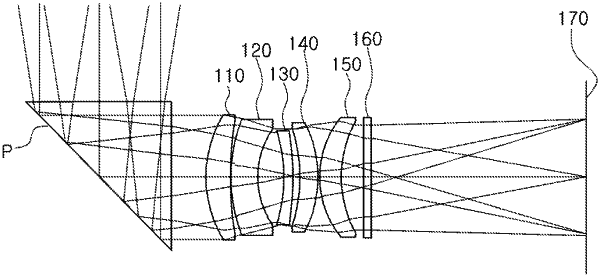
| CPC G02B 13/001 (2013.01) [G02B 9/60 (2013.01); G02B 9/62 (2013.01); G02B 13/002 (2013.01); G02B 13/0045 (2013.01); G02B 13/0065 (2013.01); G02B 27/0025 (2013.01); G03B 17/17 (2013.01)] | 11 Claims |

|
1. An optical imaging system comprising:
a first lens having positive refractive power;
a second lens having negative refractive power;
a third lens having negative refractive power;
a fourth lens having refractive power; and
a fifth lens having refractive power; and
an image sensor disposed on an image side of the fifth lens such that the fifth lens is a lens disposed most adjacent to the image sensor,
wherein the first to fifth lenses are sequentially disposed from an object side of the optical imaging system to an image side of the optical imaging system,
wherein the optical imaging system includes a total of five lenses, and
wherein 1.3<TTL/BFL<3.5 is satisfied, where TTL is a distance from an object-side surface of the first lens to an imaging plane of the image sensor, and BFL is a distance from an image-side surface of the fifth lens to the imaging plane of the image sensor.
|