| CPC G01N 21/645 (2013.01) [G02B 6/124 (2013.01); H01L 27/14825 (2013.01); G01N 15/1436 (2013.01); G01N 2021/058 (2013.01); G01N 2021/6482 (2013.01); G01N 2021/6484 (2013.01); G02B 2006/12107 (2013.01); G02B 2006/12138 (2013.01)] | 15 Claims |

|
1. An apparatus comprising:
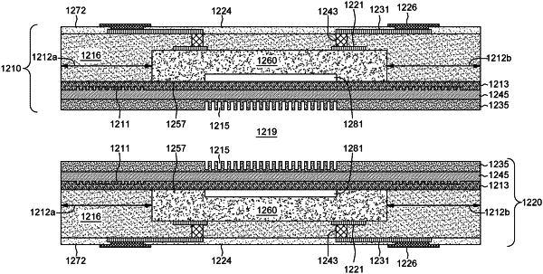
a molding layer over a substrate and covering sides of a light detection device, wherein the molding layer comprises a first region adjacent to a first edge of an active surface of the light detection device and a second region adjacent to a second edge of the active surface of the light detection device, wherein the first region, the second region, and the active surface of the light detection device form a contiguous surface;
a waveguide integration layer between the contiguous surface and a waveguide, wherein the waveguide integration layer comprises optical coupling structures on portions of a top surface of the waveguide integration layer over the top surface of the first region, and over the top surface of the second region, wherein the optical coupling structures couple light waves from a light source to the waveguide;
the waveguide over the waveguide integration layer, wherein the waveguide utilizes the light waves from the waveguide integration layer to excite light sensitive materials in one or more nanowells; a nanostructure layer over the waveguide, the nanostructure layer comprising the one or more nanowells, wherein the one or more nanowells are formed on one or more locations on the nanostructure layer, wherein each location of the one or more locations shares a vertical axis with a location on the active surface of the light detection device; and
a top layer over the contiguous surface, wherein the top layer and the active surface collectively form a space over the nanostructure layer, the space defining a flow channel, wherein the top layer comprises:
a second molding layer below a second substrate and covering sides of a second light detection device, wherein the second molding layer comprises a first region adjacent to a first edge of an active surface of the second light detection device and a second region adjacent to a second edge of the active surface of the second light detection device, wherein the first region of the second molding layer, the second region of the second molding layer, and the active surface of the second light detection device form a second contiguous surface;
a second waveguide integration layer between the second contiguous surface and a second waveguide, wherein the second waveguide integration layer comprises optical coupling structures on portions of a top surface of the second waveguide integration layer below the top surface of the first region of the second molding layer, and below the top surface of the second region of the second molding layer, wherein the optical coupling structures on the portions of the top surface of the second waveguide integration layer couple light waves from the light source to the second waveguide;
the second waveguide below the waveguide integration layer, wherein the second waveguide utilizes the light waves from the second waveguide integration layer to excite light sensitive materials in one or more additional nanowells; and
a second nanostructure layer below the second waveguide, the second nanostructure layer comprising the one or more additional nanowells, wherein the one or more additional nanowells are formed on one or more locations on the second nanostructure layer, wherein each location of the one or more locations on the second nanostructure layer shares a vertical axis with a location on the active surface of the second light detection device.
|