| CPC G01K 15/005 (2013.01) [H04N 23/11 (2023.01); H04N 25/77 (2023.01); G01J 2001/444 (2013.01); G01S 7/497 (2013.01)] | 8 Claims |

|
1. An imaging device, comprising:
a pixel array unit including pixels;
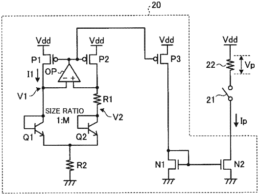
an analog signal generation unit configured to generate an analog signal based on a temperature around the pixel array unit;
an analog to digital (A/D) conversion unit configured to convert the analog signal into a digital signal;
a switch configured to cut off the analog signal to be supplied to the A/D conversion unit; and
a correction unit configured to calculate a parameter of a correction calculation expression for correction of the digital signal based on a first digital signal obtained through A/D conversion from the analog signal cut off by the switch and based on a second digital signal obtained through the A/D conversion from the analog signal generated by the analog signal generation unit.
|