| CPC G01J 1/44 (2013.01) [H04N 25/40 (2023.01); H04N 25/76 (2023.01)] | 17 Claims |

|
1. A vision sensor comprising:
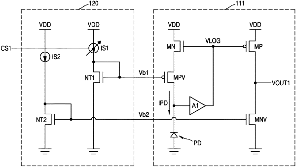
a pixel array comprising a plurality of pixels comprising a first pixel; wherein the first pixel comprises a sensing circuit configured to generate a first output voltage based on an internal voltage generated based on changes in intensity of light, and generate a second output voltage based on a first test bias voltage received from a bias voltage generation circuit, and wherein the sensing circuit comprises:
a photoelectric conversion element configured to generate a photocurrent based on the changes in the intensity of the light;
a current-voltage conversion circuit comprising a first transistor connected to the photoelectric conversion element, the current-voltage conversion circuit configured to convert the photocurrent into the internal voltage; and
a source-follower configured to convert the internal voltage to the first output voltage,
wherein the first transistor is configured to receive the first test bias voltage, and
wherein the photocurrent flows through the first transistor.
|