| CPC C23C 14/083 (2013.01) [C23C 14/3485 (2013.01); C23C 14/35 (2013.01)] | 20 Claims |

|
1. A method of forming an optical device, the method comprising:
disposing an optical device substrate on a substrate support in a process volume of a process chamber, the optical device substrate having a first surface;
forming a first optical layer on the first surface of the optical device substrate during a first time period when the optical device substrate is on the substrate support, wherein
the first optical layer comprises a metal-containing oxide, a metal-containing nitride, or a metal-containing oxynitride, and
the first optical layer is formed without an RF-generated plasma over the optical device substrate;
forming a second optical layer with an RF-generated plasma on and in contact with the first optical layer during a second time period when the optical device substrate is on the substrate support, wherein
the first optical layer is disposed between the optical device substrate and the second optical layer,
the second optical layer is spaced apart from the optical device substrate in a first direction,
the second optical layer comprises a metal-containing oxide, a metal-containing nitride, or a metal-containing oxynitride,
the first optical layer and the second optical layer consist of a single metal and one or more of oxygen and nitrogen,
the single metal is selected from the group consisting of titanium (Ti), niobium (Nb), silicon (Si), tantalum (Ta), aluminum (Al), chromium (Cr), ruthenium (Ru), hafnium (Hf), magnesium (Mg), zirconium (Zr), molybdenum (Mo), tungsten (W), manganese (Mn), iron (Fe), cobalt (Co), nickel (Ni), copper (Cu), zinc (Zn), gallium (Ga), tin (Sn), bismuth (Bi), antimony (Sb), gadolinium (Gd), and yttrium (Y),
the first optical layer has a thickness in the first direction between an atomic layer and about 10 nm, and
the second optical layer has a thickness in the first direction of greater than about 20 nm; and
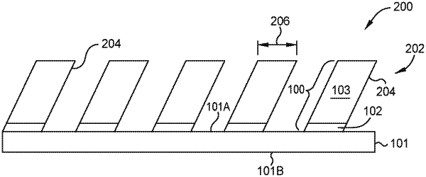
forming a plurality of optical device structures over the substrate, the plurality of optical device structures spaced apart from each other in a second direction that is perpendicular to the first direction, wherein each optical device structure includes a portion of the first optical layer and a portion of the second optical layer.
|