| CPC C03C 17/366 (2013.01) [C03C 17/3644 (2013.01); C03C 2217/21 (2013.01); C03C 2217/256 (2013.01); C03C 2217/268 (2013.01); C03C 2217/281 (2013.01)] | 6 Claims |

|
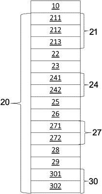
1. A low-e coating applied onto a glass for providing neutrality when viewed from inside and from outside in automotive and architectural glasses, comprising outwardly from the glass:
a first dielectric structure comprising a first dielectric layer, a second dielectric layer and a first seed layer; wherein the first dielectric layer is SixNy and a thickness of the first dielectric layer is between 15 nm and 50 nm; the second dielectric layer is TiOx and a thickness of the second dielectric layer is between 1.3 nm and 4.5 nm; and the first seed layer is ZnAlOx and a thickness of the first seed layer is between 10 nm and 30 nm;
a first functional layer positioned on said first dielectric structure, wherein a thickness of the first functional layer is between 5 nm and 22 nm;
a first barrier layer comprising NiCrOx and positioned on said first functional layer, wherein a thickness of the first barrier layer is between 0.8 nm and 2.8 nm;
a second dielectric structure positioned on said first barrier layer comprising a third dielectric layer and a second seed layer; wherein the third dielectric layer is ZnSnOx and a thickness of the third dielectric layer is between 40 nm and 70 nm; and the second seed layer is ZnAlOx and a thickness of the second seed layer is between 15 nm and 35 nm;
a second functional layer positioned on said second dielectric structure, wherein a thickness of the second functional layer is between 5 nm and 22 nm;
a second barrier layer comprising NiCrOx and positioned on said second functional layer, wherein a thickness of the second barrier layer is between 0.8 nm and 2.8 nm;
a third dielectric structure positioned on said second barrier layer comprising a fourth dielectric layer and a third seed layer; wherein the fourth dielectric layer is ZnSnOx and a thickness of the fourth dielectric layer is between 35 nm and 65 nm; and the third seed layer is ZnALOx and a thickness of the third seed layer is between 10 nm and 35 nm;
a third functional layer positioned on said third dielectric structure, wherein a thickness of the third functional layer is between 5 nm and 22 nm;
a third barrier layer comprising NiCrOx and positioned on said third functional layer, wherein a thickness of the third barrier layer is between 0.8 nm and 2.8 nm; and
an upper dielectric structure positioned on said third barrier layer comprising a fifth dielectric layer and an upper dielectric layer; wherein the fifth dielectric layer is ZnSnOx and a thickness of the fifth dielectric layer is between 10 nm and 35 nm; and the upper dielectric layer is SiOxNy and a thickness of the upper dielectric layer is between 10 nm and 35 nm;
wherein the visible region transmittance value after thermal process is between 60-75% and the solar transmittance value is between 23-35%.
|