| CPC H10N 50/80 (2023.02) [H10B 51/30 (2023.02); H10B 53/30 (2023.02); H10B 61/00 (2023.02); H10B 63/00 (2023.02); H10N 50/01 (2023.02); H10N 50/10 (2023.02); H10N 70/011 (2023.02); H10N 70/231 (2023.02); H10N 70/841 (2023.02)] | 20 Claims |
|
1. A device, comprising:
a first layer of insulating material;
a via in the first layer of insulating material; and
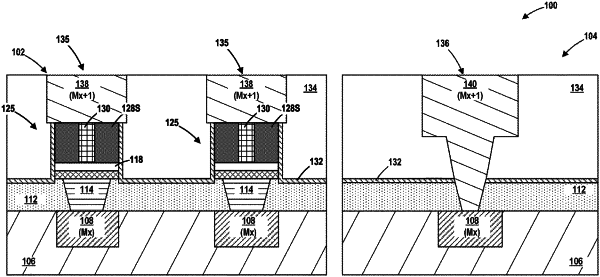
a memory cell in a first opening within a second insulating layer above the first layer of insulating material, the memory cell above the via, the memory cell including:
a bottom electrode above and in physical contact with the via, wherein the bottom electrode is within the first opening and above the first layer of insulating material;
a memory state material above the bottom electrode;
an internal sidewall spacer within the first opening, above at least a portion of the memory state material, and defining a spacer opening, the internal sidewall spacer including an upper surface perpendicular to opposing sidewalls and a bottommost surface having a first surface area; and
a top electrode within the spacer opening and above a portion of the memory state material, the top electrode including a bottommost surface having a second surface area less than the first surface area,
wherein the bottom electrode, the memory state material, and the internal sidewall spacer each have vertically aligned sidewalls.
|