| CPC H10B 12/37 (2023.02) [G11C 5/10 (2013.01); H01L 23/528 (2013.01); H01L 23/5226 (2013.01); H01L 28/60 (2013.01)] | 20 Claims |
|
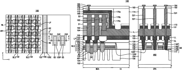
1. A semiconductor device comprising:
a substrate extending in a first direction and a second direction perpendicular to the first direction, and including a cell area having a first active region and a peripheral circuit area having a second active region;
a direct contact contacting the first active region in the cell area;
a bit line structure disposed on the direct contact;
a capacitor structure electrically connected to the first active region;
a gate structure disposed on the second active region in the peripheral circuit area;
lower wiring layers disposed adjacent to the gate structure and electrically connected to the second active region;
upper wiring layers disposed on the lower wiring layers;
a wiring insulating layer disposed between the lower wiring layers and the upper wiring layers; and
upper contact plugs connected to at least one of the lower wiring layers and the upper wiring layers and extending through the wiring insulating layer in a third direction perpendicular to the first direction and the second direction,
wherein the upper contact plugs includes a first upper contact plug that extends through the wiring insulating layer and extends through at least a portion of the upper wiring layers and the lower wiring layers.
|